Pre-Compliance Resources to Help Your Wireless Device Design Meet Regulatory Mandates
Electronic Products 제공
2016-05-18
Your assignment is to engineer a wireless link, such as Wi-Fi® or ZigBee®, for use in a small product. Putting aside the traditional design considerations of cost, board space, or power consumption, you know you'll also have to deal with the regulatory compliance mandates of the FCC in the U.S. (and comparable agencies in other regions) which affect all wireless devices. You have three basic ways to implement the link:
- Build the transceiver from "scratch" using components selected from many vendors
- Use a reference design employing the vendor's components and their suggested BOM
- Use an approved, certified "canned" module which you drop into your design; it has a data interface on one side and the antenna port on the other.
Clearly, option #1 is the most challenging, but sometimes a preferred choice; option #2 is much easier with fewer likely headaches, although implementation, layout issues, and interactions can affect performance and compliance. Option #3 is the easiest, with the highest level of confidence and shortest time to market, and compliance should be a "no-brainer," right?
Wrong. Even if the chosen module is fully approved, the final design in which it is used is not, and will need to pass certification tests. Issues such as antenna type and placement, power rail EMI, and other factors can result in failing the costly, time-consuming-type certification process and test, even with a validated module (Figure 1).
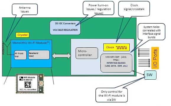
Figure 1: Even with a fully approved regulatory-compliant module, there are many things that can go wrong in the final board design and thus cause test "fail" results.
Use pre-compliance tests as a precursor
Compliance tests are expensive in terms of setup, engineering time, understanding the requirements of the FCC (or other) regulations, how the tests are performed, travel, and more. In short, it is a formal, exhaustive, and time-consuming exercise. A failing grade at this stage of product development can mean often expensive re-design and product-introduction delays while the source (or sources) is found and fixed.
Rather than just show up for the tests after doing some rough in-house measurements, companies are increasingly doing pre-compliance tests with specialized test equipment to first do the full set of tests on their own, at their own or a local site, to find out if they will pass—and if not, why not, and what to do about it. They may also hire a compliance consultant who can guide them through the test protocol and advise on solutions depending on shortcomings or failures identified in this pre-compliance testing. The goal is to uncover potential problems early and reduce risk of failing at the compliance-test stage.
Test-equipment vendors have recognized the value of pre-compliance in-house testing and developed powerful, specialized instruments which make it practical. They have developed "mixed-domain" instruments which integrate a GHz-range oscilloscope, spectrum analyzer, logic analyzer, and protocol analyzer in one unit (Figure 2, showing a design under test based on the Microchip MRF89XA module), to be used with a user-provided PC.
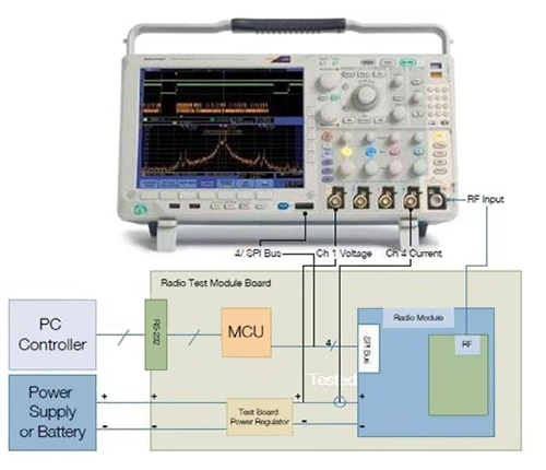
Figure 2: The test connection between the device under test (here based on a Microchip transceiver module) and a mixed-domain oscilloscope. (Image courtesy of Tektronix)
However, these mixed-domain units are not just four instruments housed in a single enclosure. The four instruments are internally linked by physical connections (no need for multiple test leads) and system firmware, so it can acquire and analyze time-correlated analog, digital, and RF signals. For example, this allows the engineer to see the effect of a change in a signal, bias setting, or state on the analog or logic side of the design with the resultant RF spectrum.
Among the compliance-related tests which these instruments and their software suite can set up and then perform are Transmit Power, Power Spectrum Density, Occupied Bandwidth, Spectrum Emission Mask, and Spurious Emission measurements, as well as Error Vector Magnitude (also called Transmit Constellation Error), each with the many good/bad masks of the compliance. They even include a near-field RF probe which can be used for "sniffing" to localize the source of undesired radiated RF, as shown in Figure 3 (in an ironic challenge to debug, such near-field emissions can actually cause subtle far-field emissions and thus non-compliance).

Figure 3: A near-field probe is used with the test instrument to pinpoint the source of undesired, troublesome RF emissions which can directly cause non-compliance, or have an indirect ripple effect and move the apparent problem elsewhere.
Compliance problems need a variety of solutions
Regulatory compliance tests and debugging are difficult. There are five stages in the challenge:
- Discover that you have a problem, and its nature.
- Capture the problem: probe, trigger, and capture it consistently if possible (tough to do, but important).
- Search and localize the problem in your data record or screens, and any correlations that may provide insight or clues.
- Analyze to see what may be causing it, via the chain and sequence of events.
- Plan, try, and test specific solutions to the apparent source(s) of the problem.
If the source of the problem is software based (such as the software keeping a signal "on" for longer than it should be, or slewing a carrier's frequency too quickly and thus creating excessive out-of-band emissions), then modifying the software is often the best approach. Sometimes, however, the software-based fix causes other problems, or is simply not possible. If the shortcoming is better handled by a hardware-centric solution, three types of add-on components are among the many options available.
Shielding against RF EMI using a metal can or enclosure may seem like an inelegant solution, but it is effective, low-cost, and can be added"after the fact" with minimum impact on the layout's design in many cases. Shields can be custom-made, of course, but a large selection of standard shields is available off the shelf.
For example, Laird Technologies offers a wide range with different appearances (solid versus "open") and lengths, widths, and height dimensions, to fit over both commonly used modules as well as sections of a PCB. Their BMI-S-101 (Figure 4) is a one-piece surface-mount shield which measures 0.476 × 0.538 × 0.1 inches high (12.10 × 13.66 × 2.54 mm).
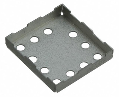
Figure 4: Standard metal shield "cans" such as this one from Laird Technologies can be a technical, cost-, and time-effective way to solve an EMI problem in RF subcircuits.
Even "simple" products such as shields have many mechanical variations in a given size. They are offered with folded, rigid, or seamless-drawn corners for different attenuation ratings (and cost), with different mounting options (through-hole or surface mount), and materials/finishes for different environments (consumer, commercial, and Mil-Spec environments). Depending on frequency, fabrication, and attachment choice, the BMI-S-101 can provide RF attenuation between 50 and 120 dB. Also, there is no penalty of power dissipation when using a metal shield.
Sometimes, compliance failure is not due to the RF circuitry itself, but the DC rail supplying the wireless subsystem. This can be a result of DC rails picking up RF emissions from elsewhere on the circuit board and then acting as mini-antennas and re-radiating them, or the DC rail and its DC/DC regulator/converter being a source of EMI/RFI due to its switching topology.
For the former case, passive ferrite beads may be an attractive EMI-suppression component. These beads are inserted in lines which are radiating energy instead of conveying it, require no additional wiring, and have no power consumption or DC dissipation (their only dissipation in this case is the RF energy which they are suppressing).
Ferrite beads come in a wide range of sizes with different attenuation ratings and frequency ranges. (Chip ferrite beads are effective for frequencies ranging from a few MHz to a several GHz.) They have inductances of microhenries in their lower-frequency range, but at higher frequencies the resistive component of the inductor produces the primary impedance (Figure 5). When inserted in series in the noise-producing circuit, the resistive impedance of the inductor prevents noise propagation.

Figure 5: The equivalent circuit model of the innocuous ferrite bead shows it is actually a resistor in series with an inductor.
There are many suppliers of ferrite beads, among them Murata Electronics. Their EMIFIL DC EMI-suppression filters are available as components with integral wire leads for PC insertion, or in versions which can be slipped over an existing wire (Figure 6 shows the Murata BL01, Murata BL02RN1, Murata BL02RN2, and Murata BL03RN2). Their performance graph (Figure 7) shows that their resistive impedance (R) increases sharply to about 200 MHz, while the inductive part of the impedance (X) stays relatively flat to the same frequency.

Figure 6: Ferrite beads such as these in the Murata BL01/02/03 series are available as slip-on components or as leaded devices, in single- as well as dual-series configurations for additional attenuation and physical-layout options.
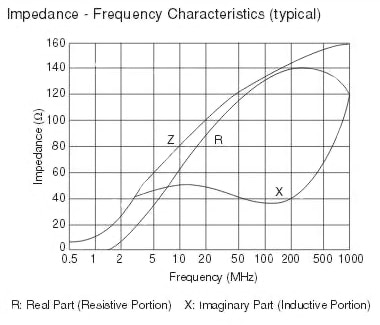
Figure 7: Even seemingly simple components such as those in the Murata BL01/02/03 have a Z = R + jX impedance versus frequency graph which reveals useful and needed design information.
For situations where the DC/DC switching regulator is the source of excessive EMI, some designers opt to use a spread-spectrum approach. In this topology, the DC/DC regulator does not operate at a fixed frequency; instead, the frequency is deliberately varied (dithered) in a pseudorandom pattern around a nominal setting.
The result is not that they generate less RF energy, but the energy that is generated is "spread" across a wide spectrum and so does not exceed the regulatory maximum in any part. Note that some engineers consider this technique to be an inelegant "cheat" while others feel it is quite legitimate for addressing the problem.
A representative device is the LTC3543 from Linear Technology, a synchronous step-down buck regulator with integral PLL which provides up to 600 mA with user-selectable spread-spectrum functionality. Its 2.5 V to 5.5 V input-voltage range makes it a good fit for applications powered by a single Li-Ion battery.
It has a nominal fixed-operating frequency of 2 MHz, but that can be set to spread across the band from 1 MHz and 3 MHz. The result is a significant reduction in peak RF noise of about 20 dB (Figure 8), with the unspread peak at about 2.3 MHz and the spread-spectrum peak at 2.5 MHz. The apparent 20 dB attenuation can easily make the difference between failing and passing the requisite compliance mandates.
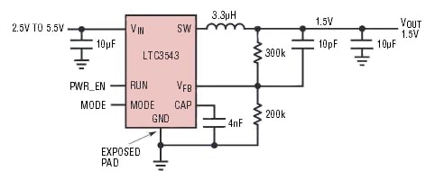
Figure 8: The LTC3543 DC/DC step-down buck regulator from Linear Technology has user-switchable spread-spectrum functionality, which can reduce the noise energy in specific parts of the RF spectrum, while not reducing the total noise energy.
In summary, RF and wireless-link designs can be relatively easy if using a purchased module, or be fairly challenging by using a do-it-yourself design. Regardless of the approach chosen, meeting the increasingly stringent regulatory compliance requirements limiting out-of-band emissions and other undesirable attributes in all operating modes is a difficult task requiring advanced insight and experience.
Specialized test equipment can help clarify the nature of the problem and locate its sources. Components such as basic metal shielding, EMI-suppressing ferrite beads, and energy-spreading DC regulators are among the hardware solutions to consider.
For more information about the parts discussed in this article, use the links provided to access product pages on the DigiKey website.
면책 조항: 이 웹 사이트에서 여러 작성자 및/또는 포럼 참가자가 명시한 의견, 생각 및 견해는 DigiKey의 의견, 생각 및 견해 또는 DigiKey의 공식 정책과 관련이 없습니다.


