Solving the RF Power-Detection Challenge
Electronic Products 제공
2016-04-01
Most RF devices must monitor and also control their RF power output to comply with government regulations, minimize RF interference, and minimize power use. Transmitters also do this for obvious reasons: 1) to minimize transmit power to increase run time and 2) to minimize power dissipation.
For the received signal path, RF power detection is also a critical function. It’s needed to monitor received RF power to adjust gain, where an RSSI (received signal-strength indicator) is used to control the gain of the RF/IF signal chain via an AGC (automatic gain control) circuit in order to maintain a constant, optimized signal level for subsequent analog-to-digital conversion (if any) and demodulation. The RSSI signal is also used to control the transmit channel, so as to minimize transmit power while also maintaining an acceptable minimum BER (bit-error rate). For these reasons, accurate RF power detection is important in both receivers and transmitters.
Note that this RF power detection differs from RF power measurement, although there is some confusion, ambiguity, and overlap in the terminology. RF power detection is generally used to refer to the measurement of the RF power (usually as a relative value) as represented by a voltage (and current) within an electronic circuit; in contrast, RF power measurement is direct measurement of the power (usually as an absolute value) of the RF wireless signal in space or air.
For the former situation, various ICs and modules are used within a circuit; for the latter, specialized sensors (often based on thermocouples) intercept the impinging RF energy and then convert its heat energy to a voltage corresponding to the RF power. [Recall that power and energy are intimately related parameters: energy is the time integral of power, while power is the time derivative of energy, the rate at which energy is being received or sourced.]
There are three architectures used to solve the problem of RF power detection, and they are usually implemented with RF ICs (although in some specialized cases, modules or hybrid techniques must be employed): root mean square (RMS), logarithmic (log), and Schottky peak (also called envelope). Each involves different internal circuitry, of course. From the user perspective, each has performance attributes which make it a better solution for a certain range of frequencies, response times, and signal shapes, as well as cost and power issues. Regardless of type, all RF power detectors have detailed data sheets with numerous graphs detailing performance across a wide range of variations in key parameters.
RMS power detection
An RMS power detector produces a DC voltage that is linearly proportional to the log of root mean square (RMS) input power, with a straightforward scaling of mV/dB. These detectors have high linearity, often better than ±1 dB across a 40 dB range, and can operate into the GHz range. A well-designed RMS-measurement IC can provide accurate RF power readings to within ±0.2 dB, even with waveforms that have content with a high crest factor (the ratio of peak to RMS value of the signal).
This makes these detectors a good fit for solving the challenge of assessing RF power when measuring complex waveforms found in spread spectrum CDMA/W-CDMA, OFDM, WiMax, and higher-order QAM modulation systems, which can have crest factors of 10 to 15 dB. Such waveforms are found in LTE, 3G, 4G, and 5G wireless devices, primarily smartphones, and especially the cellular base stations (which have requirements that are more demanding than the phones themselves).
A representative RMS detector is the LT5581 from Linear Technology Corp., which operates from 10 MHz to 6 GHz with 40 dB dynamic range and targets wireless standards such as GSM/EDGE, CDMA, CDMA2000, W-CDMA, TD-SCDMA, UMTS, LTE, and WiMAX, among others. It outputs a DC voltage in linear scale proportional to an RF input signal power in dBm. The RMS detector uses a proprietary technique to accurately measure the RF power from –34 dBm to +6 dBm (at 2.14 GHz) of modulated signals with a crest factor as high as 12 dB.
Figure 1 shows LT5581 used as a power-amplifier level control over the full operating range, using a directional coupler as the power pickoff. Since the types of waveforms it is monitoring will have different crest factors, the vendor supplies a graph showing error versus crest at various power levels (Figure 2).
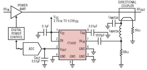
Figure 1: The LT5581 RMS RF detector can be used to assess RF PA power from 10 MHz to 6 GHz, here shown using a directional coupler between the PA output and the antenna input.
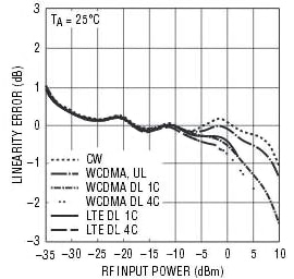
Figure 2: As the LT5581 is used with a wide range of signal types, and performance is dependent on the crest factor of the signal being monitored, the data sheet shows its linearity with various signal formats over a wide frequency range.
Log power detection
Logarithmic amplifier detectors (sometimes called successive-detection log video amplifiers) provide a DC output voltage that is log-linearly proportional to its input power level; they are not responding to the RMS value. They are well suited to measure signals with wide dynamic range, on the order of up to 100 dB, from DC to microwave frequencies. They offer very high sensitivity and so they are a good match for very low signal levels. Accuracy is in the range of ±0.2 dB, compatible with the needs of both RSSI and TSSI (transmit-signal-strength indicator) functions. For pulsed RF signals, the log type may be a good choice because of its fast response times (on the order of nsec).
Log detectors solve another problem, that of determining circuit gain. This usually requires dividing the output power reading by the input reading. Doing so is a difficult enough operation for high-speed analog circuits, but completely impractical via numeric computation processing due to the signal frequencies. The input and output would have to both be digitized, then extremely high-speed computational effort used; even if technically possible, it would be costly and dissipate considerable power. However, when two logarithmic detectors are used, the power gain of a circuit can be measured by subtracting the input-signal reading from the output reading, which can be done using a simple analog-subtraction circuit.
An example of this type of power detector is the LMV225 from Texas Instruments (Figure 3), intended for use in CDMA and WCDMA applications from 450 MHz to 2 GHz. Its output is an accurate temperature- and supply compensated voltage which is linearly related to input power, in dBm, over a 30 dB dynamic range. In a typical application, it is used for PA power control (Figure 4). Typical of RF power detectors, the data sheets include numerous basic performance curves as well as graphs showing behavior due to parameter variations (Figure 5).
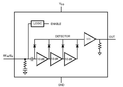
Figure 3: The LMV225 log detector is composed of three 10 dB stages, for a total range of 30 dB.
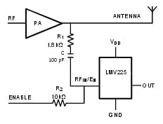
Figure 4: A common application of the LMV225 is to measure the relative output of a transmit-chain power amplifier, via a small RC impedance-matching network.
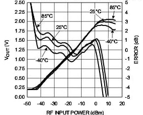
Figure 5: The plot of the LMV225 output voltage and log performance versus RF input power at 2 GHz shows the complexity of RF-detector characterization.
Peak detection
RF Schottky peak (envelope) detectors combine a temperature-compensated peak detector based on a Schottky diode and buffer amplifier in a small package. This is the high-frequency RF embodiment of the classic analog-peak detector, a simple circuit (in principle) which requires only a diode, buffer amplifier, and small-value hold capacitor to track a signal’s “envelope” and so provide an output which is the peak value of that envelope.
In an RF-optimized version, the input voltage’s peak is detected using an on-chip Schottky diode for lowest voltage drop and fastest response; and the detected voltage is buffered and appears at the amplifier output. This detector is well-suited to applications such as radar, where the shape of the receive signal is less important than its peak value, which provides information such as the target type and radar cross section. It also is often chosen to solve problems in TSSI/RSSI circuits, power amplifier (PA) linearization, and wideband power monitoring.
The peak detector has a very fast response, which is also critical because many radar signals (and thus their return echoes) transmit very short pulses to minimize the signal “shadow period” during which the received echo is obscured by the transmit pulse. Primary applications include electronic warfare, intelligence, and countermeasures, as well as broadband test and measurement.
The Maxim MAX2204 is a peak detector which operates from 450 MHz to 2.5 GHz (Figure 6), with an output voltage which increases monotonically with increasing input power, over a detection range of -16 dBm to +5 dBm. The tiny SC-70 5-lead IC compensates for temperature and process shifts, yielding output variation of less than ±0.5 dB at full-input power and less than ±1.5 dB at the lower power. It also features a response time of several hundred microseconds (Figure 7), commensurate with wireless and cellular applications (note that peak detectors for high-performance radar systems have response times which are several orders of magnitude faster, but with much higher power dissipation and cost).
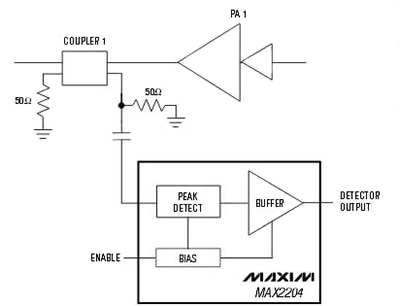
Figure 6: The Maxim MAX2204 RMS power detector features a detection range from -16 dBm to +5 dBm.
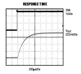
Figure 7: The response time of the MAX2204 is well-matched to the needs of wireless devices employing standards which operate in the 450 MHz to 2.5 GHz range.
Regardless of the RF power detector type selected, temperature performance is always an important consideration for two reasons. First, they use analog components such as diodes, which have an inherent temperature coefficient (tempco) and thus an associated drift with temperature. Second, many RF power detectors are used in harsh applications, such as military and aerospace designs, where extreme low and high temperatures are unavoidable.
Vendors of RF power detectors minimize the tempco effect by using a combination of techniques including laser trimming of circuit elements and clever circuit topologies in which some of the drift-related errors cancel each other out. However, users of these detectors should look not only at the basic performance specification such as accuracy at nominal temperature, but also the specified performance at relevant temperature extremes.
Summary
Different RF applications have different power-detection requirements and priorities, and the objectives of a wireless communications link are very different than those of a radar system, as one example. Users of RF systems who need to detect relative power levels can choose among three main types of detector IC, usually referred to as RMS, log, and peak types. These different detectors offer varying combinations of response time, sensitivity to peak versus RMS value, dynamic range, and accuracy, to cite a few key specifications. Each type uses a very different internal circuit design and IC process.
Today’s RF ICs can provide and exceed performance that was difficult and costly to achieve just a few years ago, and in a smaller package with far-lower power dissipation. As a result, many applications which used no RF power detection, or just an approximate approach, are now able to benefit from more sophisticated and accurate techniques. In the usual product-feedback loop, where improved components drive better systems, which in turn drives demand for even-better components, today’s systems require much-higher levels of detector capabilities to achieve advanced performance with low cost, low power, and a small footprint.
For more information about the parts discussed in this article, use the links provided to access product pages on the DigiKey website.
면책 조항: 이 웹 사이트에서 여러 작성자 및/또는 포럼 참가자가 명시한 의견, 생각 및 견해는 DigiKey의 의견, 생각 및 견해 또는 DigiKey의 공식 정책과 관련이 없습니다.
